Semiconductor Inspection Using SWIR Cameras
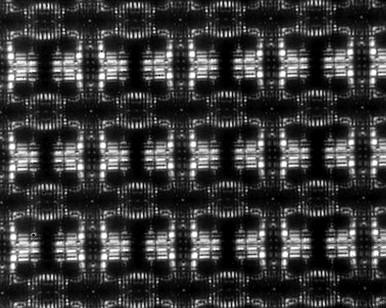
The use of Short Wave Infrared (SWIR) Cameras for inspection of silicon wafers is based on relative transparency of silicon in this portion of the spectrum. This allows users to monitor for defects within in the silicon wafer, such as fine cracks which can affect the performance of the end product manufactured from that silicon wafer.
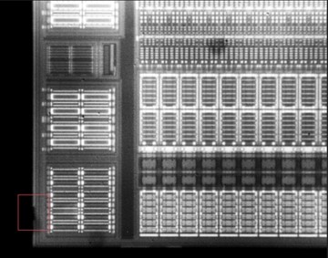
A very important process in semiconductor manufacturing is the alignment of the silicon wafer with respect to various reference points so that the next step in the wafer processing can be done with a high level of accuracy. By using SWIR Cameras to look through the wafer, internal structures or front side surface structures can be visualized from the bottom of the wafer and used for alignment purposes.
For processes that are time dependent or where the whole wafer area has to be monitored at high resolution, the Manx SQ Series (for highest resolution mapping) or Manx R Series (for highest sensitivity) can be used.
The Manx SQ and R Series have the following features:
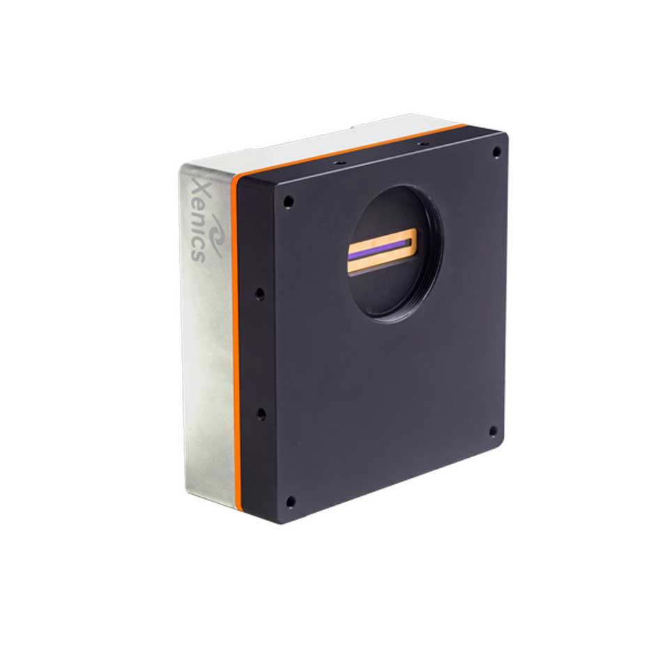
- 2048 resolution for large area coverage; SQ for highest resolution, RECT for highest sensitivity
- High speed scanning – up to 260Hz line rates
- Flexible Gain Settings – choose the optimal mode, either high sensitivity or high dynamic range
- Manx SQ Series Datasheet, Manx R Series Datasheet
- Product information/quote
For processes that are not time dependent, or when the whole wafer does not need to be imaged at high resolution, a SWIR Area Scan camera can be used.
The Wildcat 640 Series is an ideal product for this application, since it has a full size VGA sensor (640×512 pixels) and has a low readout noise. For those who are looking for a lower cost solution, the Bobcat 320 Series is also available.
The Wildcat 640 Series has the following features:
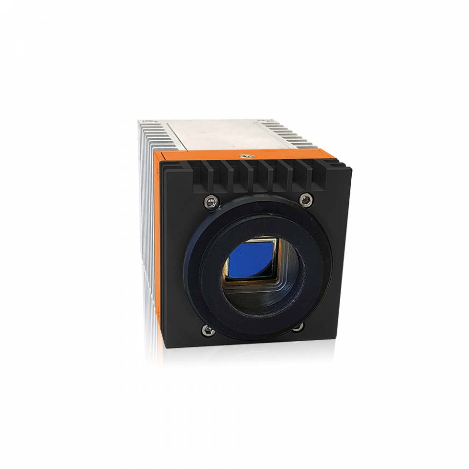
- Full Size Sensor (640×512)
- Low Readout noise
- Compact Size for easy integration into microscopy test stations
- Wildcat 640 Series Datasheet
- Product information/quote